2N5322 Transistor Pinout, Equivalent, Applications, Features and Other Details
2N5322 is a 10 Watt PNP transistor available in TO-39 package. In this post you will find 2N5322 transistor pinout, equivalent, applications, features and other details.
Absolute Maximum Ratings:
- Package Type: TO-39
- Transistor Type: PNP
- Max Collector Current(IC): 2A
- Max Collector-Emitter Voltage (VCEO): 75V
- Max Collector-Base Voltage (VCBO): 100V
- Max Emitter-Base Voltage (VEBO): 5V
- Total Power Dissipation (PD): 10W
- Max Transition Frequency (fT): 50 MHz
- Minimum & Maximum DC Current Gain (hFE): 30 to 130
- Max Storage, Operating & Junction temperature range: -65 °C to +200 °C
NPN Complementary:
The NPN complimentary of 2N5322 is 2N5320
Replacement and Equivalent:
2N5323
2N5322 Transistor Explained / Description:
2N5322 is a PNP transistor that is a part of a series which also contains 2N5320 PNP transistor. The transistor has some good features/advantages if you use it in your circuit such as the availability of its NPN which makes a pair, good storage and operating junction temperature, high collector-emitter voltage, 10W power dissipation, upto 50MHz transition frequency, general purpose usage etc.
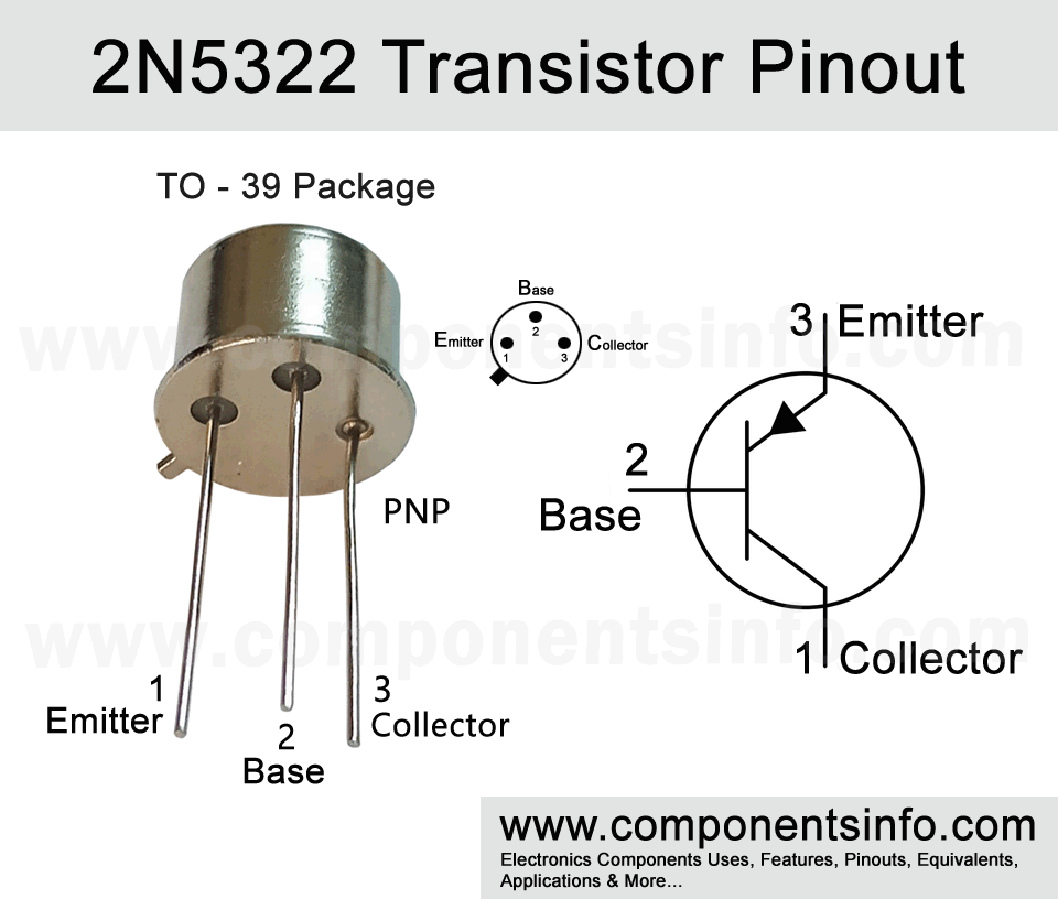
Looking at the pinout of the transistor the pin that is near the tab is pin1 Emitter, the middle pin is pin 2 Base and the last pin is Collector pin3.
The absolute maximum ratings of the transistor are as follows: The collector current is 2A, collector-emitter voltage is 75V, emitter-base voltage is 5V, collector-base voltage is 100V, total power dissipation is 10W max storage temperature range is from -65°C to 200°C and operating junction temperature is 200°C.
The transistor is designed to be used in switching and medium power amplifier applications, the detailed list of its applications can be found under the applications heading below.
Where We Can Use it & How to Use:
As mentioned this transistor is designed to be used in medium power amplifier and switching applications due to which it can be used in variety of different types of amplifiers and load driving circuits or switch circuits.
To use the transistor as a switch apply signal (signal from which you want to control the load) to its base through a current limiting resistor. The emitter pin will be connected with the positive rail of the circuit and the collector pin is connected with the positive wire of the load and the negative wire of the load will be connected with the negative rail of the circuit.
To use the transistor as an amplifier apply signal (the signal that you want to amplify) to its base through a suitable capacitor and two resistor biasing network. Connect the emitter pin with the positive rail of the circuit, and connect collector through a resistor (load resistor) to the negative rail of the circuit. The output or amplified signal will be taken where you have connected the collector and load resistor through a electrolytic capacitor.
Applications:
Audio amplifier circuits
Voltage Regulator
Motors Control
Switching circuits
Power supply
Safe Operating Guidelines:
Here are some safe operating guidelines to use the transistor.
- Always use the transistor 20% below from its absolute maximum
- The maximum collector current of the transistor is 2A so by following the above 20% rule we will use 1.6A only.
- Same as the max collector-emitter voltage is 75V but we will not drive load of more than 60V.
- Use a suitable heatsink with the transistor.
- The power dissipation should not exceed 10W.
- The transistor’s internal and external temperature should always be between this range: -65°C to 200 °C.
Datasheet:
To download the datasheet just copy and paste the below link in your browser.
https://my.centralsemi.com/datasheets/2N5320-5323.PDF