2N5952 jfet Pinout, Equivalents, Specs, Explanations, Features and More
This post contains details about 2N5952 jfet pinout, equivalents, specs, explanations, features, where and how to use it and other useful information about this transistor.
Features / Technical Specifications:
- Package Type: TO-92
- Transistor Type: N Channel JFET
- Maximum Drain to Gate Voltage: 30V
- Maximum Gate to Source Voltage: -30V
- Maximum Gate Current: 10mA
- Minimum to Maximum Gate to Source Cutoff Voltage : –1.3V to –3.5V
- Maximum Power Dissipation: 350mW
- Max Storage & Operating temperature Should Be: -55 to +150 °C
- Max Noise Figure:- 2.0dB
Replacement and Equivalent:
2N5485, 2N5457, J201, MPF102, 2SK30A, 2SK118, BF245, 2N5932
2N5952 Transistor Explained / Description:
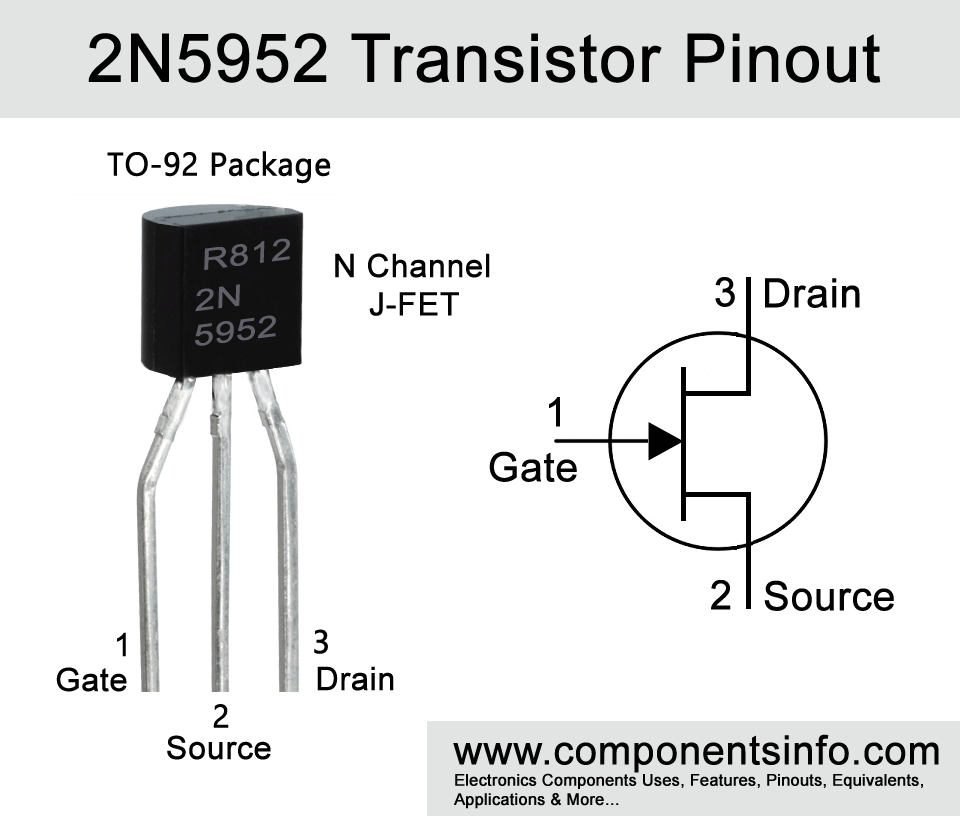
2N5952 is an N channel JFET or junction field effect transistor. The transistor is manufactured in TO-92 package and the pin configuration are as follow, when looking from the front the first pin of the transistor is Gate, second pin is Source and the third pin is Drain.
The device is primarily designed to use for electronic switching. It is a low noise transistor with the noise figure of 2.0dB. Looking at the characteristics and ratings of the transistor the maximum drain to gate voltage is 30V, the max gate to source voltage is -30V and the max forward current is 10mA. The gate reverse current is -1.0nA, gate to source cutoff voltage is -1.3 to 3.5 and the total device dissipation is 350mW.
Where and How to Use:
As mentioned above 2N5952 is primarily designed for electronic switching but it can also be used for other general purpose application which falls under its ratings and electrical characteristics. It is also used in some musical instruments such as in pedals.
Applications:
Electronic Switching
Variety of general applications
Musical Instruments
Safe Operating Guidelines / Absolute Maximum Ratings:
In order to use this transistor safely and achieve stable long-term performance with it, it is recommended not to use the transistor at its absolute maximum rating and always keep it 20% below from its max ratings. Using the transistor to its absolute maximum ratings can result in damage to the transistor, shorten its life, or impair its performance.
The maximum drain to source voltage is 30V therefore do not drive load of more than 24V. The maximum forward gate current is 10mA therefore do not drive load of more than 8mA and always store or operate the transistor at temperature above -55°C and below +150 °C.
Datasheet:
To Download the datasheet just copy and paste the below link in your browser.
https://cdn.datasheetspdf.com/pdf-down/2/N/5/2N5952-FairchildSemiconductor.pdf


