2SA1962 Transistor Pinout, Equivalent, Features, Uses and Other Useful Info
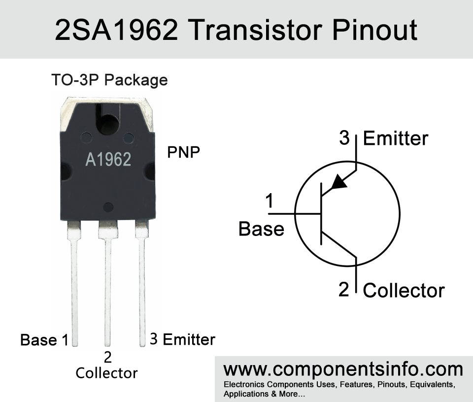
2SA1962 is a PNP power amplifier transistor available in TO-3P package. In this post we will discuss 2SA1962 transistor pinout, equivalent, features, uses and other useful information.
Absolute Maximum Ratings:
- Package Type: TO-3P
- Transistor Type: PNP
- Max Collector Current(IC): –15A
- Max Collector-Emitter Voltage (VCE): –230V
- Max Collector-Base Voltage (VCB): –230V
- Max Emitter-Base Voltage (VEBO): –5V
- Max Collector Dissipation (Pc): 130 Watt
- Minimum & Maximum DC Current Gain (hFE): 55 To 160
- Max Storage & Operating temperature: -55 to +150 Centigrade
NPN Complementary:
NPN Complementary of 2SA1962 is 2SC5242
Replacement and Equivalent:
2SA1987, HA1962, 2SA1986
2SA1962 Transistor Explained / Description:
2SA1962 is a TO-3P package PNP transistor mainly designed to be used in power amplifiers and Audio output amplifiers of high fidelity type but it is not limited to these applications and can also be used in other applications. The transistor has many good features such as good collector current, high collector-emitter voltage, transitions frequency of 3MHz, DC current gain of 55 to 160, good collector power dissipation and availability of its complimentary pair.
The absolute maximum ratings of the transistor are as follows: The collector-emitter voltage is -230V, collector current is -15A, collector-base voltage is -230V, emitter-base voltage is -5V, base current is -1.5A, collector power dissipation is 130W, junction temperature 150°C and storage temperature is from -55°C to 150°C.
The transistor is available in two different types according to its DC current gain and can be identified by the alphabet written after its part number. If the alphabet is “R” then its DC current gain or hFE value will be 55 to 110 and if that alphabet is “O” then its hFE value will be 80 to 160.
How to Use Transistor:
Although the transistor is designed to be used as an amplifier but it is not limited to that and can also be used as a switch. To use it as a switch apply signals to its base pin (The signals through which you want to control the output load). It is must to use a current limiting resistor between the signal source and the base pin of the transistor. You can use a current limiting resistor value between 1K to 10K.
The Emitter pin of the transistor will be connected with the positive rail of the circuit and the load will be connected between collector and the negative rail of the circuit.
To use the transistor as an amplifier apply the signals which you want to amplify to its base pin through a coupling capacitor you can use an electrolytic capacitor. Connect the emitter pin with the positive rail of the circuit and the amplified output will be taken from the collector.
It is to be that this is a very simple way to make an amplifier circuit and to enhance it you have to use many other passive components.
Applications:
Audio Amplifier Stages
HiFi Audio Amplifiers
DC to DC Converters
Switching Regulators
Inductive Load switching
Battery Management Systems
PWM Circuits
Switching load of up to 10A
Safe Operating Guidelines:
Here are some important guidelines to safely operate the transistor.
- For safe operating always use the transistor 20% below from its absolute maximum ratings.
- Check pin layout before use.
- Use a heatsink with the transistor.
- Storage and operating temperature should be between -55°C to +150°C.
Datasheet:
To download the datasheet just copy and paste the below link in your browser.
https://www.alldatasheet.com/datasheet-pdf/view/30042/TOSHIBA/2SA1962.html


