BC309 transistor Pinout, Features, Equivalent, Applications, Where and How to Use and More
This post explains BC309 transistor pinout, features, equivalent, applications, where and how to use and other related information of this PNP bipolar junction transistor or BJT.
Absolute Maximum Ratings:
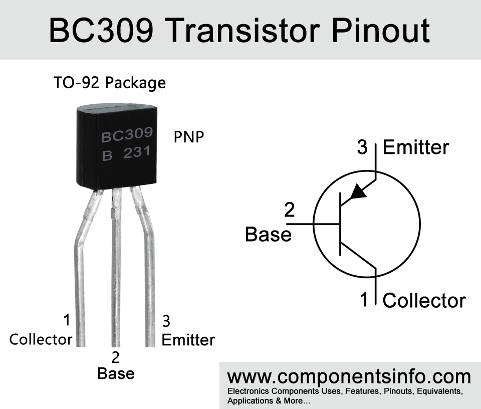
- Package Type: TO-92
- Transistor Type: PNP
- Max Collector Current(IC): -100mA
- Max Collector-Emitter Voltage (VCEO): -25V
- Max Emitter-Base Voltage (VEBO): -5V
- Max Collector Power Dissipation (Pc): 500 milliwatt
- Max Transition Frequency (fT): 130 MHz
- Minimum & Maximum DC Current Gain (hFE): 120 – 800
- Max Storage & Operating temperature Should Be: -55 to +150 Centigrade
NPN Complementary:
NPN Complementary of BC309 is BC239
Replacement and Equivalent:
BC556, BC557, BC560 (Before using these alternatives it is suggested to check the pin layout.)
BC309 Transistor Explained / Description:
If you are looking for a high gain and low noise general purpose transistor for your applications then BC309 can be a good candidate. It is a PNP transistor and is available in TO-92 package. It is a part of the BC30x series which also contains other transistor such as BC307 and BC308.
The transistor possesses good noise figure from typically 2 to maximum 4dB and minimum to maximum DC current gain of 120 to 800. Moreover, the maximum transition frequency of 130MHz also makes it ideal to use in many types of high frequency and RF circuits.
Understanding the pin layout of the transistor, the first pin is “Collector”, Second pin is “Base” and the Third pin is “Emitter”.
The absolute maximum ratings of the transistor are as follows:
The max collector current is -100mA, max emitter-base voltage is -5V, max collector-emitter voltage is -25V, max collector power dissipation is 500mW, maximum junction temperature is 150°C and the maximum storage temperature is from -55°C to 150°C.
The transistor is available in three different versions according to its DC current gain or hFE and can be determined by the alphabet written after the part number. If the alphabet is “A” then the gain will be 120 to 220, if “B” then the gain will be 180 to 460 and if “C” then its gain will be 380 to 800.
Where We Can Use it & How to Use:
BC309 is designed to use for amplifier and switching applications. But it can also be used in other applications such as signal amplification, audio preamplification etc. and due to its good electrical characteristics this transistor can be used in RF circuits also. As it is a BJT transistor so using procedure will be same as you use other PNP BJT transistor by providing the signal on its “Base” pin getting output from the “Collector” pin and connecting the “Emitter” pin with the ground. (Some passive components will be necessary according to the requirement for example current limiting resistor at Base etc.
Applications:
Audio Amplifier Stages
Signal Amplification Circuits
Darlington Pairs
Audio Preamplifier Circuits
RF Circuits
Sensor Circuits
Switching Loads under 100mA
Safe Operating Guidelines:
Below are the safe operating guidelines of the transistor.
- Do not use the transistor to its absolute maximum ratings and always stay 20% below from these ratings.
- Check the pinout before placing it in your circuit.
- So according to the 20% below usage guideline above the maximum collector current is -100mA but we will only use -80mA.
- The maximum collector-emitter voltage is -25V but we will stay under 20V.
- The maximum storage temperature is from -55°C to 150°C, so we have to save the transistor from temperatures below and above these limits.
- Moreover, the junction temperature should not go above 150°C.
Datasheet:
To download the datasheet just copy and paste the below link in your browser.
https://www.mouser.com/datasheet/2/308/BC309-1190467.pdf