BC635 Transistor Pinout, Features, Equivalent, Applications and More
BC635 is a quite interesting transistor with lot of good features packed in a TO-92 package. In this post we are going to discuss BC635 transistor pinout, features, equivalent, applications, where and how to use and other details about this NPN BJT.
Absolute Maximum Ratings:
- Package Type: TO-92
- Transistor Type: NPN
- Max Collector Current(IC): 1A
- Max Collector-Emitter Voltage (VCEO): 45V
- Max Emitter-Base Voltage (VEBO): 5V
- Max Base Current (IB): 100mA
- Max Collector Power Dissipation (Pc): 1W
- Max Transition Frequency (fT): 100 MHz
- Minimum & Maximum DC Current Gain (hFE): 25 – 250
- Max Storage & Operating temperature Should Be: –65 to +150 Centigrade
PNP Complementary:
PNP Complementary of BC635 is BC636
Replacement and Equivalent:
BC637, BC639, BC639-16, 2SD1207, C3940, 2N6731, ZTX853, ZTX692B, ZTX455, S8050DA, NTE2341, MPS455, CS9103C.
BC635 Transistor Explained / Description:
BC635 is an interesting transistor with a lot packed in a TO-92 package such as a collector current of up to 1A, max DC current gain of 250, and a transition frequency of 100MHz.
It is an NPN BJT transistor from the series of BC63x transistors. The series also contains two other transistors which are BC637 and BC639, these two transistors of the series can easily be replaced with BC635 because they have higher voltage characteristics than BC635. Complimentary transistor series of these transistors is also available so you can use them where you require the complimentary transistor of each to make a pair. The complementary transistors of these are BC636, BC638 and BC640.
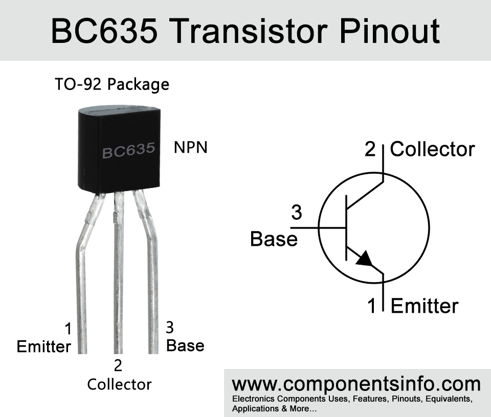
Looking at the pin configuration of the transistor when looking from the front (part number side) the first left pin (pin1) is “Emitter”, the middle pin (pin2) is “Collector” and the last pin (pin3) is Base.
The absolute maximum ratings of the transistor are as follows:
The maximum collector-emitter voltage is 45V, maximum emitter-base voltage is 5V, maximum collector current is 1A, max base current is 100mA, max collector power dissipation is 1Watt, max junction temperature is 150°C and max storage temperature is from -65°C to 150°C.
Where We Can Use it & How to Use:
The transistor is designed to be used in amplifications and switching applications but due to its good electrical characteristics it can also be used in other applications such as Radio and RF circuits, sensing circuits, analog computation applications, signal amplifying etc. It is a BJT transistor and can be used the same as you use other BJT transistors by applying signal to its base, connecting emitter to the negative connection of the circuit, and connecting collector with the load’s negative side and the positive side of the load will be connected with the positive connection of the circuit. Of course, you have to use other discrete components such as resistors and capacitor where it is required.
Applications:
Sensor Circuits
Signal Amplification Circuits
Audio Amplifier Circuit
Audio Amplifier Stages
Darlington Pairs
Radio Circuits (Around 100MHz)
Transmitter Circuits (Around 100MHz)
Active Filters
PWM Circuits (For Small Motors and Other Loads)
Switching Loads under 1A
Safe Operating Guidelines:
Here are the safe operating guidelines of the transistor.
- Always use the transistor 20% below from its absolute maximum ratings.
- So according to the 20% below usage guideline the maximum collector current is 1A but we will only drive load under 0.8A max.
- Max collector-emitter voltage of the transistor is 45V but we will not drive load of more than 36V.
- Make sure to use and store the transistor at temperatures above -65°C and below 150°C.
Datasheet:
To download the datasheet just copy and paste the below link in your browser.
https://www.mouser.com/datasheet/2/149/bc635-294174.pdf