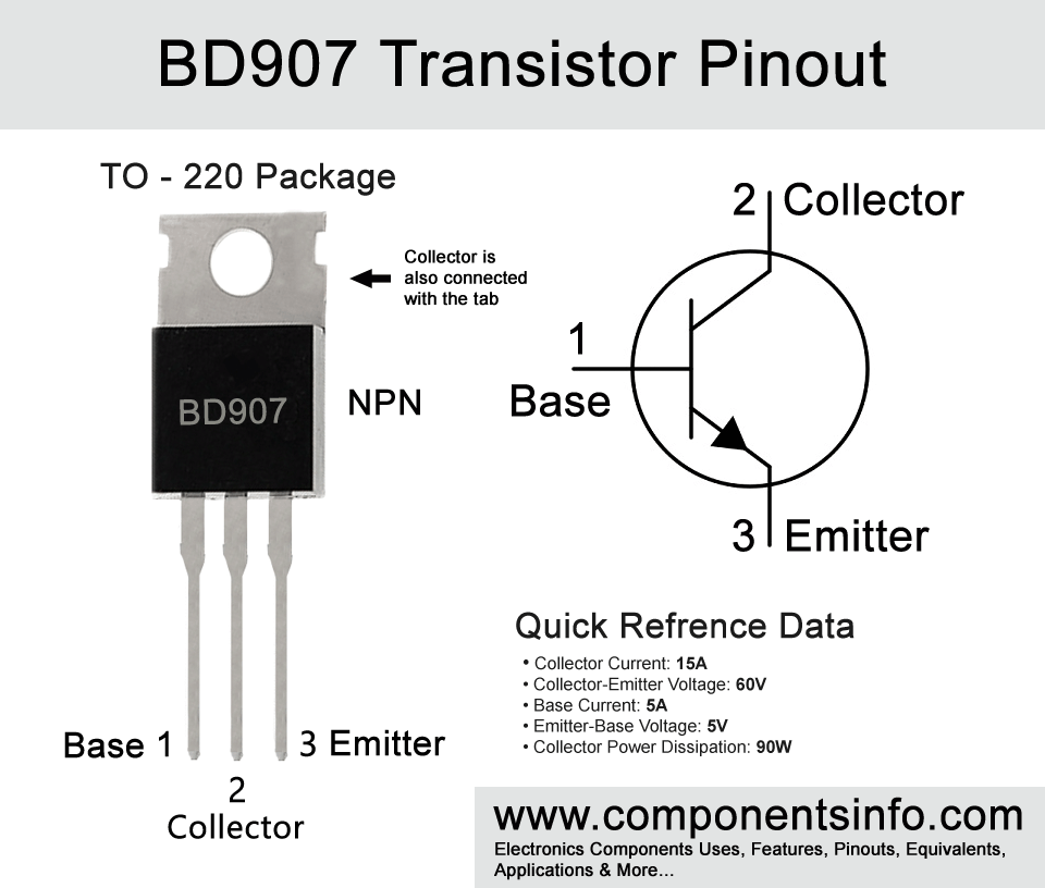
BD907 Transistor Pinout, Equivalents, Features, Applications, Safe Operating Guidelines and More
BD907 is a TO-220 package NPN transistor, in this post we are going to understand BD907 transistor pinout, equivalents, features, applications, safe operating guidelines and other details about this component.
Absolute Maximum Ratings:
- Package Type: TO-220
- Transistor Type: NPN
- Max Collector Current(IC): 15A
- Max Collector-Emitter Voltage (VCEO): 60V
- Max Emitter-Base Voltage (VEBO): 5V
- Max Base Current (IB): 5A
- Max Collector Power Dissipation (Pc): 90W
- Minimum & Maximum DC Current Gain (hFE): 40
- Max Storage & Operating temperature Should Be: -65°C to 150°C
PNP Complementary:
PNP Complementary of BD907 is BD908
Replacement and Equivalent:
BD909, BD911, BD743A/B/C/D
BD907 Transistor Explained / Description:
BD907 is an NPN BJT or bipolar junction transistor designed to be used in switching and amplifier applications of general purpose type. It is a transistor of a series which also contains other transistors such as BD905, BD909 and BD911. All the transistor in the series can be used alternatively in low voltage applications under 45V but above this voltage range you have to choose the one that has more collector-emitter voltage than your applications requirements.
The absolute maximum ratings of the transistor are collector current is 15A, emitter-base voltage is 5V, collector-emitter voltage is 60V, emitter-base voltage is 5V, base current is 5A, maximum power dissipation is 90W and max storage and operating temperature is from -65°C to 150°C.
As mentioned above the transistor is designed to be used in general purpose switching and amplifier applications but its good absolute maximum ratings and the electrical characteristics makes this transistors capable to use in wide variety of applications such as power supply circuits, battery related circuit, controller circuits etc. The detailed list of its applications can be found below under the applications heading.
How to Use:
To use the transistor as a switch apply signal to its base through a suitable resistor. Connect the collector with the negative supply of the load and the positive supply of the load will be connected to the positive rail of the circuit. Connect emitter pin with the ground or negative rail of the circuit.
To use it as an amplifier fed the signal to its base through a coupling capacitor and also use a biasing network of two resistors one side of each resistor is connected to the base and other side of one resistor will be connected to the positive rail of the circuit and one side of another resistor will be connected negative rail of the circuit. The emitter pin will be connected to the negative rail of the circuit through a resistor with a capacitor that will be used paralleled with that resistor. The collector of the transistor will be connected with the positive rail of the circuit through a resistor and the output will be connected with the collector of the transistor.
Applications:
Inverters
Audio Amplifiers
Telecommunication
Voltage regulators
DC-DC Converters
Power Supplies
Battery Charger Circuits
Lighting Control Circuits
Motor Controller Circuits
Converters
Safe Operating Guidelines:
Here are the safe operating guidelines of the transistor.
- Always use the transistor atlease 20% below from its absolute maximum ratings.
- The maximum collector current is 15A but according to the above rule of 20% we will only use 12A.
- Same as the maximum collector-emitter voltage is 60V but we will not use more than 48V.
- Use a suitable heatsink.
- Always Store and operate the transistor between 65°C and below 150°C.
Datasheet:
To download the datasheet just copy and paste the below link in your browser.
https://www.alldatasheet.com/datasheet-pdf/view/262346/ISC/BD907.html