BDX53C Transistor Pinout, Equivalent, Features, Applications and Other Useful Data
In this post we are going to discuss BDX53C transistor pinout, equivalent, features, applications and other useful information such as where and how to use etc.
Absolute Maximum Ratings:
- Package Type: TO-220
- Transistor Type: NPN Darlington
- Max Collector Current(IC): 8A
- Max Collector-Emitter Voltage (VCEO): 100V
- Max Collector-Base Voltage (VCBO): 100V
- Max Emitter-Base Voltage (VEBO): 5V
- Max Collector Power Dissipation (Pc): 60 Watt
- Minimum DC Current Gain (hFE): 750
- Max Storage & Operating temperature: -65 to +150 Centigrade
PNP Complementary:
PNP Complementary of BDX53C is BDX54C
Replacement and Equivalent:
NTE2343, NTE263, TIP132, TIP102, MJF6388, BDX33D, BDX33C, BDW93C, BDW73C, BDW42, BDT65B/C, BDT65B/C, BD901, BD649, 2SD1196, 2N6532, HP102, 2SD1123
BDX53C Transistor Explained / Description:
If you are looking for a medium power transistor for variety of general purpose application in your lab or looking for a better medium power transistor for your projects then BDX53C can be a good choice. The transistor can drive load of upto 8A and can supply upto 100V to the load.
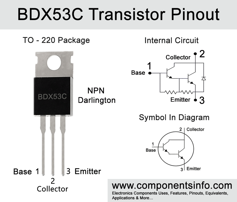
Looking at the package of the transistor, it is made in TO-220 package and the pin configuration of the transistor are: first pin is Base second is Collector and the third is Emitter. Now understanding the transistor internally or looking at its internal diagram it is a darlington transistor containing two transistors with two resistors and a diode. The darlington is the name of a pair of two transistors connecting in a way (showed in the internal circuit in the transistors pinout image above) that amplifies the output gain to a great extent which makes the transistor useful to use in applications that require high gain output or control a load with a low level signal.
Now looking at the absolute maximum ratings of the transistor the maximum continuous collector current is 8A, maximum collector to emitter voltage is 100V, maximum collector to base voltage is also 100V, maximum emitter-base voltage is 5V and maximum collector power dissipation is 60 Watts.
Where We Can Use it & How to Use:
The transistors can be used in amplifier, switching, power liner and Driver applications but it is not limited to these applications and can also be used in wide variety of other applications which are mentioned under the applications heading below.
To use the transistor first of all it is important to understand what voltage and current is required by your load. Also please note that your load should be 20% below from the absolute maximum ratings of the transistor.
After that check the pin configuration of the transistor and connect the Emitter pin with the negative supply of the circuit, connect Base with the input signal you want to amplify or from which you want to control the load and connect the Collector with the load (If the transistor is used as a switch) or use it as an output of the amplified signal (If it is used as an amplifier). For making a better amplifier you have to use the required passive components to get the required gain and audio quality.
Applications:
Audio Amplifiers
Motor Control
Switching Circuits
Voltage Regulation
Pulse Generator
Voltage inverters
LED Drivers
DC to DC Converters
Battery Operated Applications
Safe Operating Guidelines:
Operating guidelines of the transistor are as follows.
- To get better performance with the transistor it is important to not drive it at its absolute maximum ratings and stay at least 20% below from these max ratings.
- So according to the above 20% below driving procedure the max collector current this transistor is capable of is 8A but we will not go above 6.4A.
- The maximum collector to emitter voltage is 100V but according to the 20% rule we will stay under 80V.
- And the storage and operating temperature of the transistor should be maintained between -55°C to 150°C.
Datasheet:
To download the datasheet just copy and paste the below link in your browser.
https://datasheetspdf.com/pdf-down/B/D/X/BDX53C_FairchildSemiconductor.pdf


